Saving energy, speeding up drug development and creating unbreakable information security
The Quantum Networks group aims at exploring quantum information science at the nanoscale and developing novel quantum photonic devices. Such quantum devices are central for quantum information networks, quantum computation and quantum cryptography systems, and lie at the basis of the forthcoming Quantum Internet. We focus on quantum control and manipulation of novel nanostructures at the single-photon and single-electron level, using nanowires, quantum dots, and hybrid atomic-solid state systems.
Quantum computers are already just around the corner. Yet, the most advanced quantum computers today exploit superconducting qubits, which, unfortunately, do not have a native photonic interface, so they cannot be interconnected.
The qNet group is committed to creating a robust technological platform for making solid-state multi-qubit devices with a photonic interface that could become a platform for a quantum network, facilitate truly 100% secure communications, and save us a lot in energy costs.
One of our key milestones is the exploration and demonstration of a novel location qubit, based on crystal-phase quantum dots. Here we aim to attain designable and scalable quantum systems grown with atomic precision, followed by a multi-qubit register with a photonic interface. These quantum registers will then be used in a prototype application of a quantum information network, or the quantum Internet, the likes of which has never been seen before!
We believe that these new advancements along with the eventual creation of quantum networks, would trigger the transformation of countless industries.
Nanowire quantum dots
Quantum dots are among the most promising candidates for various photonic systems in quantum technology. Embedding quantum dots in nanowires boosts these systems with a set of powerful possibilities, such as precise positioning of the emitters, excellent photon extraction efficiency and direct electrical contacting of quantum dots. Notably, nanowire structures can be grown on silicon substrates, allowing for straightforward integration with silicon-based photonic devices. Here we have developed the growth of GaAs quantum dots in AlGaAs nanowires on silicon. We precisely control the dimensions of quantum dots and their position inside nanowires and demonstrate that the emission wavelength can be engineered over the range of at least 30 nm around 765 nm. Our nanowire quantum dots have excellent optical properties, and we now explore this system for advanced photonic devices based on multiple coupled quantum dots in a nanowire.
Multi-qubit quantum photonic devices
Semiconductor quantum dots are one of the best on-demand sources of single and entangled photons to date, simultaneously merging the highest brightness and indistinguishability of the emitted photons. They are, therefore, among the strongest candidates for practical single-qubit quantum photonic devices. However, to exploit the full advantage of quantum physics, multi-qubit photonic devices are absolutely necessary. For instance, multi-qubit quantum registers with photonic interfaces are vital in the development of the forthcoming Quantum Internet. Here we aim to realize practical multi-qubit photonic devices for quantum networks based on novel crystal-phase quantum dots in nanowires. This is a recently developed technology uniquely allowing for the fabrication of quantum devices with an ultimate precision of a single atomic layer.
Epsilon-near-zero grids for on-chip quantum networks
Realization of an on-chip quantum network is a major goal in the field of integrated quantum photonics. Here we aim to develop such networks based on novel epsilon-near-zero (ENZ) materials, exhibiting a close-to-zero relative permittivity. The great advantages of ENZ materials are that electromagnetic waves can propagate in a subwavelength waveguide with acute bends almost without reflection losses and with almost constant phase. We exploit these phenomena to demonstrate numerically that ENZ materials can strongly protect quantum information against decoherence and losses during its propagation in a dense network.
Hybrid atomic-solid state quantum systems
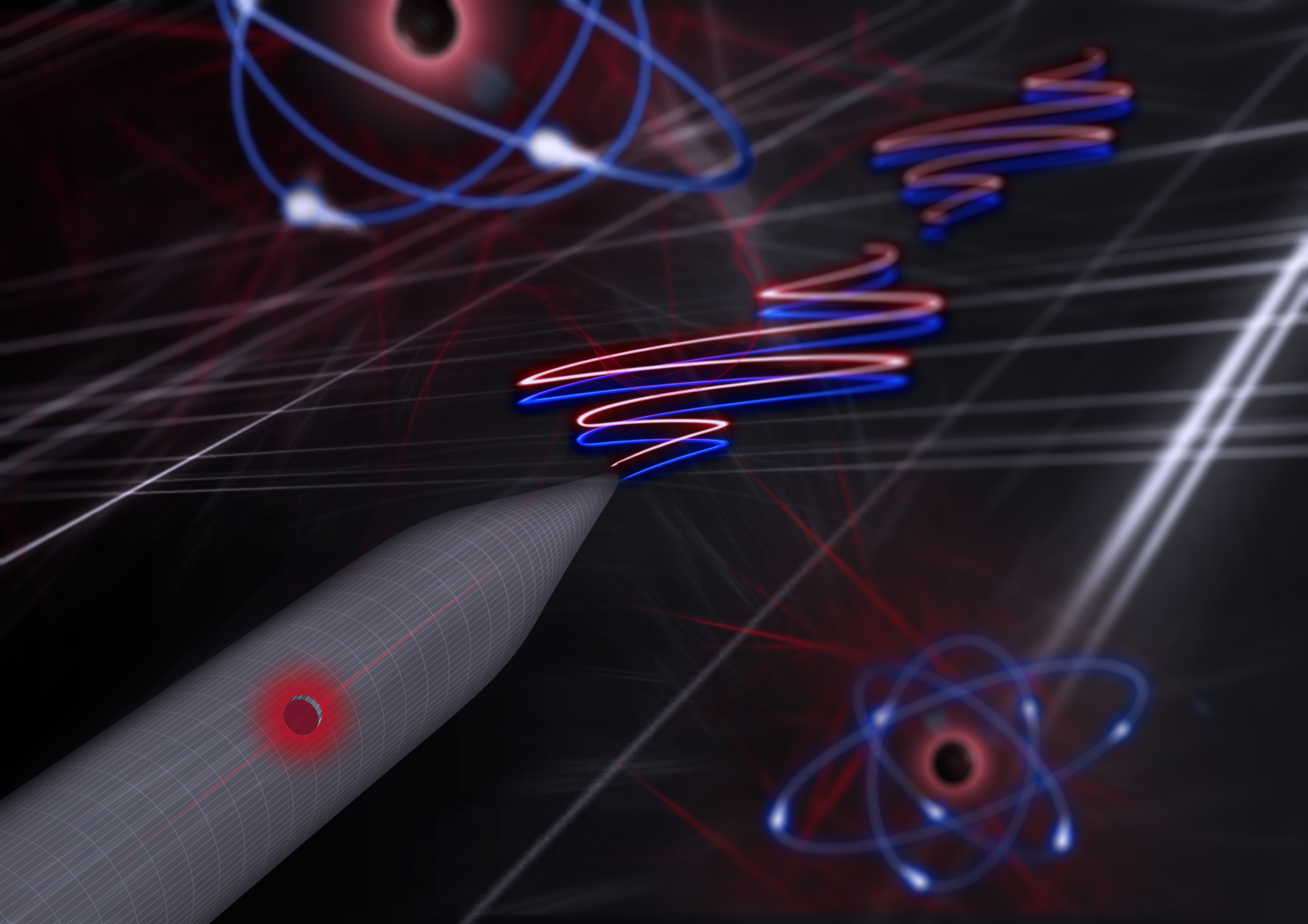
Hybrid atomic-solid state systems are promising building blocks for quantum photonic technologies because they can combine the advantages of both constituents. Here we explore such hybrid systems by coupling quantum dots and atomic vapors. Quantum dots are engineerable, scalable, tunable and deterministic sources of single and entangled photons. Atomic vapors are widely used as slow-light media and quantum memories. The coupling of single quantum dot emission to atomic vapors opens exciting new avenues where the scalability and functionality of nanostructure devices based on single quantum dots can be combined with the uniformity of atomic systems in hybrid interfaces. We have demonstrated, for instance, frequency-looking of GaAs quantum dot emission to an optical transition in Rb atoms, enabling the use of quantum dots as nodes in quantum networks. Quantum network of artificial atoms A network is formed from multiple quantum nodes located at different remote places. Quantum information is transferred from node to node by a single photon. An artificial atom (a quantum dot) coupled to natural atoms lies at the core of each node. An artificial atom represents “hardware” for a qubit, that is capable of sending, receiving and storing of quantum information. Coupling to natural atom ensures that all the nodes in the network are independently frequency-locked to the exact same optical transition of an atom. Such frequency-locking of all nodes is important because it ensures that all nodes can “talk” to each other, by sending and receiving photons of the same frequency.
Contact
Nika Akopian Group Leader, Associate Professor nikaak@dtu.dk