But there is a problem: today’s computer chips are very good at working with electricity, while generating light directly on a chip is much harder.
Now, researchers have found a new way to make a tiny, bright and stable light source directly on a silicon chip. The results, published in Science Advances, could help pave the way for faster and more energy-efficient technologies for moving data.
Here’s the twist
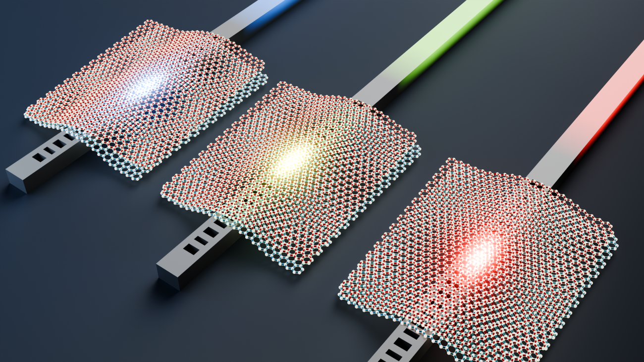
The researchers used an unusual material made from two extremely thin layers of atoms.
These materials are so thin that they are only a few atoms thick. When the two layers are stacked on top of each other with an almost perfect alignment, they form a special pattern known as a moiré superlattice.
This pattern changes how the material behaves. In particular, it helps keep the particles that produce light together for longer, making it much easier for the material to emit light efficiently.
The researchers then combined this material with a silicon nanocavity, a structure that traps light within an ultra-small space. This structure acts a little like an optical echo chamber: it strengthens the light and produces a very narrow, well-defined beam.
The light can then be guided directly into the silicon chip through a tiny optical waveguide.
A light source built for telecommunications
The new device produces light at a wavelength used in current fibre-optic communication systems, tapping directly into existing infrastructure, and it operates at room temperature, meaning you don't need to cool it to extremely low temperatures or use complicated equipment just to make it operate.
The researchers demonstrated a bright, very narrow light signal with a linewidth of around 0.2 nanometres. Think of this as light with a very precise colour. The more precisely defined the light is, the easier it is to use for transmitting information reliably. It’s a sign that the source produces high-quality, well-controlled light. And to top it off? The light can be efficiently guided into the chip's optical circuitry, bringing researchers a step closer to putting complete light-based communication systems onto a single tiny chip.
This is important because most optical communication systems currently rely on separate light sources. Being able to build the light source directly into the chip could make future photonic systems smaller, more compact and potentially more energy-efficient.
Why the tiny twist matters
Different technologies need light at different wavelengths, and one of the most interesting features of this approach is that researchers can change the properties of the light by changing how the two atomic layers are aligned.
That gives scientists a new way to control the colour – or wavelength – of the light produced by the material, while the integration with silicon photonics connects these material properties with established photonic components.
In the future, different combinations of ultra-thin materials, different layer alignments and techniques such as stretching the material could make it possible to tailor tiny on-chip light sources to different technologies, without having to redesign the entire chip.